If you have any problems with material analysis, please feel free to contact us.
Our analysis services at NTT Advanced Technology (NTT-AT) leverage the materials analysis expertise cultivated over many years at NTT Laboratories, and we specialize in the analysis of semiconductor and fuel cell-related materials, cleanroom environment assessment, and analysis related to telecommunications infrastructure equipment.
We support our customers' research and development with a diverse range of services tailored to their specific needs.
Detection sensitivity and size of analytical methods (image)
If you hover the mouse over the name of each analysis method in the figure below, the target size of that analysis will be displayed. Click to go to the details page for each analysis.
* It may not work properly on smartphones and tablets.
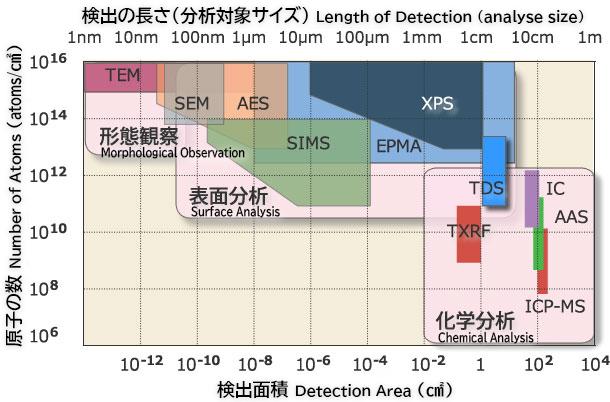
Morphological observation
Device, material morphology/structure, composition evaluation
Search by analysis method
| Analysis method | Information obtained | Application example | Surface resolution |
|---|---|---|---|
| TEMs transmission electron microscope |
Cross-sectional structure | Cross-sectional observation of semiconductor devices, FFT | 0.2nm |
| FIB-SEM | Information such as internal voids and defects | Defect analysis of porous ceramics | |
| SEM scanning electron microscope |
Observation of surface shape | Detailed shape observation of defective parts | 2nm |
| AFM atomic force microscope |
Observation of surface microscopic unevenness | Silicon micro-roughness measurement | several nanometers |
surface analysis
Any analysis requires "know-how," including measurement conditions and sample preparation. Our strength lies in proposing the optimal analytical method tailored to the customer's analytical objectives, sample condition, resolution, detection sensitivity, and other various conditions, and performing analyses that reflect the true information of the sample.
Search by analysis method
| Analysis method | Information obtained | Application example | analysis element and Detection limit concentration |
depth resolution and Surface resolution |
|---|---|---|---|---|
| SIMS Secondary ion mass spectrometry |
I want to obtain the concentration of impurities with high sensitivity. | Dopant depth distribution | H~U ppb~ppm |
A few to several tens of nm 1 to several tens of μm |
| XPS X-ray photoelectron spectroscopy |
Surface composition and chemical state | Surface oxidation state, surface contamination | Li~U 0.1~1% |
>2nm >30μm |
| AES Auger electron spectroscopy |
Structure depth information Elemental analysis of minute parts |
Structure of thin film, qualitative analysis of contaminants | Li~U 0.1~1% |
>2nm >15nm |
chemical analysis
Main holding equipment
Search by analysis method
| Analysis method | Information obtained | Application example | analysis element | Detection limit concentration |
|---|---|---|---|---|
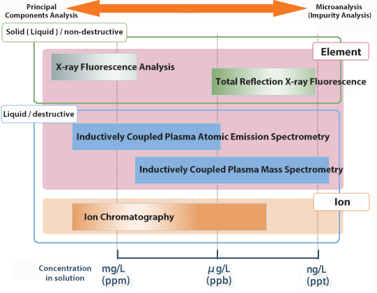
| ICP-QQQ Triple quadrupole inductively coupled plasma mass spectrometry |
High sensitivity elemental analysis ・Solution analysis ・Fracture analysis |
Analysis of trace metals on Si wafers, trace metals in the environment, and impurities in pure water | Elements other than halogen, inert gas, H, C, N, O | Sub ppt ~ (Depends on the object being measured) |
| I C Ion chromatographic analysis |
Analysis of highly sensitive solutions Qualitative and quantitative analysis of ions |
Clean room atmosphere survey | anions, cations, organic acid ions | ppt to ppm (depending on measurement target) |
| TXRF Total reflection X-ray fluorescence analysis |
High sensitivity elemental analysis ・Non-destructive ・Non-contact |
Wafer surface contamination Compound semiconductors other than Si substrates (sapphire, SiC, GaN, etc.) |
Na~U | 109atoms/cm2~1010atoms/cm2 |
| GC-MS gas chromatograph mass spectrometry |
Qualitative and quantitative analysis of organic compounds, Structural analysis |
Identification of organic compounds, structure determination, organic matter analysis during CR | Elements other than halogen, inert gas, H, C, N, O | ppb~ (depending on measurement target) |
| XRF X-ray fluorescence analysis |
Elemental analysis | Thin film/powder/bulk composition qualitative analysis | B~U | ~0.01% |
| ICP-AES ICP emission spectrometry |
trace elemental analysis, Multi-element analysis |
Composition analysis of various materials and thin films | Elements other than halogen, inert gas, H, C, N, O | ppb~ (depending on measurement target) |
Test Characterization
We evaluate and measure the optical properties of optical communication materials, gas permeability, viscoelasticity, thermophysical properties, and powder properties of materials.
Search by analysis content
| Analysis content | Information obtained |
|---|---|
| gas permeability | (Gas/water vapor) permeability |
| Viscoelasticity | Dynamic viscoelasticity (tension, bending, torsion), melt viscoelasticity |
| thermophysical properties | Glass transition point of material, heat value/weight change |
| Powder properties | Specific surface area (BET method), particle size distribution (laser diffraction method/dynamic light scattering method), pore distribution |
| Endotoxin analysis (displays an external site in a new window) | endotoxin concentration |
Analysis Flow
At NTT-AT 's materials analysis center, we don't just provide analytical data; we work together with our customers to understand their problems and propose the most suitable solutions.
Step 1 Inquiry(problem submission)
If you have any problems with material evaluation, please feel free to contact us! Please feel free to contact us via the inquiry form or by phone. Please tell us the sample name, sample shape, composition, etc. to the extent possible.
Step 2 Submit your idea
We will propose the optimal analysis method based on the customer's problem, sample, etc. We will conclude a confidentiality agreement upon request.
Step 3 Examining ideas
Our customers' requests (needs) for material evaluation extend beyond simple material analysis to include everything from new material development to process reliability evaluation.
Step 4 Estimate & Plan(Proposal)
We will provide you with an estimate of delivery date, fees, schedule for analysis, etc. If a trial is required, we may conduct a trial analysis in advance.
Step 5 contract
If you have any questions about the quotation, please feel free to contact our sales representative. After placing your order, we will conduct an analysis.
Step 6 Result report
After conducting the analysis, we will deliver the analysis results report along with the delivery note and receipt. Upon request, we will notify you of the results by email prior to delivery.
Step 7 Payment
Please stamp the receipt attached at the time of delivery and return it. We will charge you an analysis fee. As a general rule, payment will be made by bank transfer at the end of the month of the following month.
Please contact us first.
Our analysis services help customers solve various problems.
Please contact us using the contact button on the bottom right.
*If your request is from overseas, we may not be able to respond to your request due to transportation or technology export issues.
Location Information
Inside the NTT Atsugi R&D Center (Click here for a map)
Location 3-1 Morinosato Wakamiya, Atsugi City, Kanagawa Prefecture 243-0124
Nearest station Hon-Atsugi Station / Aiko-Ishida Station (Odakyu Line)
Click here for information on other locations (headquarters, etc.)