シリコン導波路 (シリコンフォトニクス)
最先端研究開発をサポートするファウンドリーサービス
お客様の研究開発を促進し、アイディアを実現!!
弊社シリコン導波路作製サービスの特徴
お客様の設計に基づいたシリコン導波路を作製
高度加工技術に支えられたSi細線導波路ベースのプラットフォーム上にお客様の設計に基づいた極微細光回路を実現します。
※ 設計図( GDSⅡ形式 もしくは dxf 形式)をご用意ください。
シリコン導波路と光ファイバアレイ間の低損失接続を実現
スポットサイズ変換器の搭載により光ファイバなどと低損失での接続が可能となり、お客様の高精度評価を実現します。
多様な設計ニーズに対応可能
光学特性の精密制御、ポリマー等の異種材料との複合のなどお客様の多様なニーズにオプションにて対応します。
シリコン導波路の作製→特性評価→光ファイバ実装までシームレスな対応
シリコン導波路の作製のみならず、お客さま要望に基づき光学特性の評価そしてチップへの光ファイバ付け実装まで、シームレスな対応が可能です。
1. Si細線導波路 -基本的な試作チップ製作例-
Si細線導波路ベースのプラットフォーム上にお客様の設計に基づいた極微細光回路を実現します。
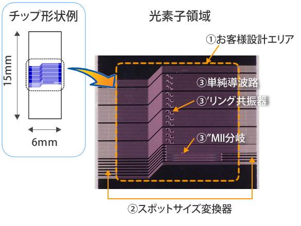
仕様例
| 導波路コア径 | 400~500nm幅×220nm厚さ |
|---|---|
| リング共振器ギャップ | 150nm以上 |
| 導波路領域 | 5mm×5mm |
| SS変換コア径 | 3μm×3μm |
| SS変換部導波路間隔 | 50μm以上 |
| チップ切出しサイズ | 15mm×5.6mm |
パッシブ導波路・光回路に対応
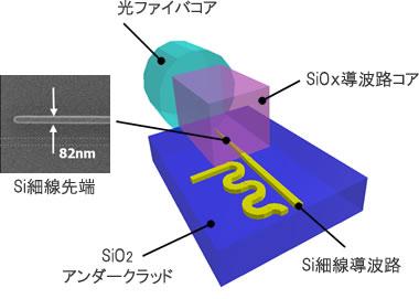
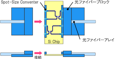
2. 低損失接続: スポットサイズ変換器
導波路端部にスポットサイズ変換を付加することで、光ファイバやレーザと低損失で接続できます。(1.5[dB/connection])
光ファイバアレイをSiチップに接続した例
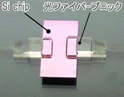
ファイバアレイの接続構造
3. オプション加工例
- 温度制御用ヒーターと配線附加
- 屈折率を高精度に制御し、透過波長を制御。
- 機能材料の導入
- 分極材料等機能材料の導入。
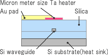
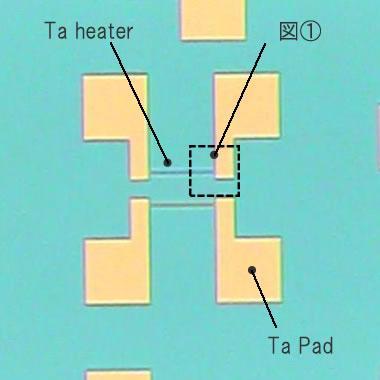
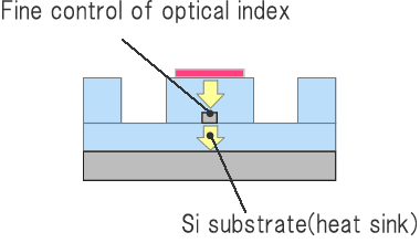
温度制御用極小Taヒーター
- 応用例
-
○光スイッチ、精密波長フィルタ
- お客様要求
-
○局所加熱による光学特性の精密制御
- 解決策
-
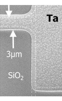
- 高融点金属のTa薄膜にすることで、切れにくいヒータを実現
- 高精度形状加工により、極微細ヒータを実現
- 低抵抗Au配線による引き回しで、特定部分のみの加熱を実現
石英(オーバークラッド)上のTaヒータパタン加工例
応用例
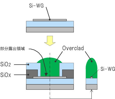
機能材料の導入
種々の機能材料を用いて、オーバークラッドが形成できます。
- 応用例
-
○センサ、変調器
- お客様要求
-
○Si導波路と機能材料をハイブリッド化
- 解決策
-
- Si導波路の部分露出構造の実現
- ドライエッチング及びウェットエッチングを組み合わせてSi導波路にダメージを与えない加工を適用
- 部分的にオーバークラッドを形成しないプロセスの実現