Fiber connection implementation service for silicon photonics
By adhesively fixing the Si waveguide chip and fiber, a high-precision stage is no longer required for chip characterization, making handling easier.
It can also be combined with a base plate or PCB board to secure the chip.
Please use this to create samples for experiments, as well as samples for display or storage.
Main service contents
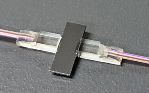
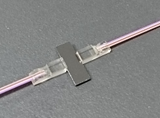
Fiber Array Connection
Adhesive fixation of the chip and fiber eliminates the need for equipment such as a high-precision stage when evaluating chip characteristics, improving the reproducibility of optical characteristics.
Optical evaluation of chips before connection
We evaluate the optical loss and spectrum of the chip. By evaluating the chip in advance, you can select the best port for fiber connection.
Combination with PCB board
Connecting the chip's electrode pattern to the PCB board with wire bonds makes it easy to evaluate the electrical characteristics.
Features of our services for Si waveguides
| Connection method | edge connection only | |
|---|---|---|
 |
 |
|
| Fiber type | single mode fiber, PANDA fiber, Small diameter fiber (MFD* approx. 4 μm), Small diameter PANDA fiber (MFD* approx. 4 μm) |
|
| Chip size | Width: 5mm~, Length: 5mm~ | |
| fiber array pitch | 127μm~ (standard 250μm) | |
| alignment wavelength | 1.55 µm | |
*For connections other than the above, please contact us.
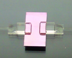
Si waveguide connection example
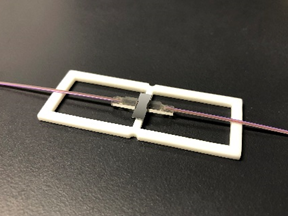
Fiber arrays are bonded to both ends of the Si waveguide chip, and are mounted in a fixed frame to prevent stress on the connections.
It is easy to handle and is convenient for evaluating various chips (electrical, temperature, and wavelength characteristics) and storing them.
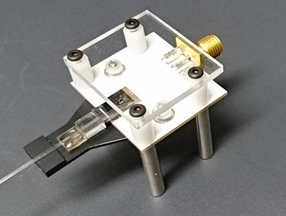
Mounting a Si waveguide on a printed circuit board facilitates the evaluation of electrical characteristics.
We also accept wire bonding processing between PCB substrates and Si waveguide chips.
Standard implementation example
| item | content |
|---|---|
| chips | Paid by customer Or you can make it yourself (Silicon waveguide) |
| fiber array | Paid by customer Or you can quote separately |
| End face | Glass application, polishing (perpendicular) |
| Alignment | Align and connect with 2 ports that allow light to pass through |
Small diameter fiber 250μm 4 cores (perpendicular to end surface)