Electro-optic crystal KTN (KTa1-xNbxO3)
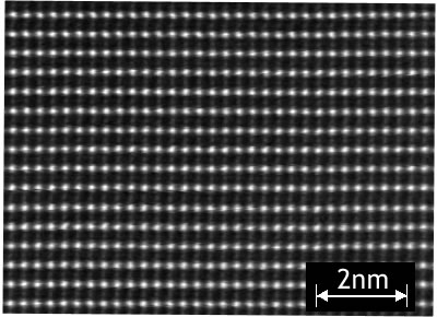
Added TEM image of KTN crystal
Overview
KTN crystals are oxide crystals composed of potassium (K), tantalum (Ta), and niobium (Nb), and possess the greatest electro-optic (EO) effect among existing materials.
This large EO effect (Kerr effect) can be used to create small, non-moving optical scanners (optical deflectors), variable focus lenses, and highly efficient phase modulators.
Our company sells optical devices using KTN crystals, such as optical scanners and variable focus lenses, as well as OCT light sources for optical scanner applications and KTN crystal chips for research and novel device applications.
For information on niobium-free oxide lens material KT (KTaO3) crystals, please see here.
feature
>> Large EO effect (s11~ = 3.0 × 10⁻¹⁵ m² / V², ex: δn~0.003 *under the conditions below)
* εr = 17500, 400 V/mm, wavelength 633 nm (according to our research)
>> Wide range of usable wavelengths
(The wavelength range in which the EO effect can be utilized is 488 nm to 3500 nm, and it is a transparent single crystal with nearly 100% internal transmittance.)
application
List of papers published by external researchers
a) Klaus C. Gwosch, Jasmin K. Pape, Francisco Balzarotti, Philipp Hoess, Jan Ellenberg, Jonas Ries and Stefan W. Hell
"MINFLUX nanoscopy delivers 3D multicolor nanometer resolution in cells",
Nature Methods, volume 17, 217-224, 2020.
b) Jasmin K. Pape, Till Stephan, Francisco Balzarotti, Rebecca Büchner, Felix Lange, Dietmar Riedel, Stefan Jakobs and Stefan W. Hell,
"Multicolor 3D MINFLUX nanoscopy of mitochondrial MICOS proteins",
Proc. Natl. Acad. Sci. USA, published August 11, 2020.
- optical modulator
- For various research (chips, devices)
*We do not guarantee that the content of the published paper meets your purpose of use or the content of the published paper.
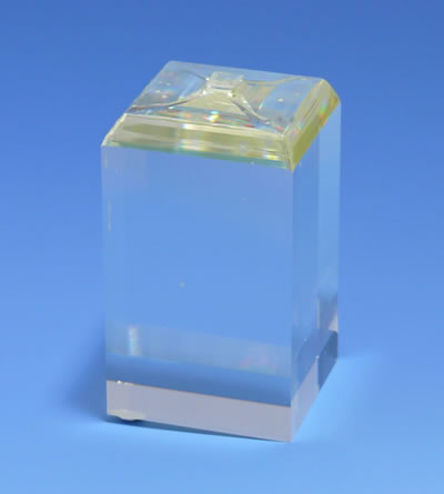
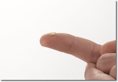
KTN crystal chip
KTN crystal chips can also be processed in terms of size and shape based on the customer's device design. Also, please feel free to contact us regarding T C (phase transition temperature), electrodes, anti-reflection coatings, etc.
The following sizes are in stock, so we can offer them at an affordable price.
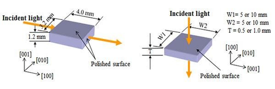
| Size (unit: mm) | Polished surface |
|---|---|
| 4.0×3.2×1.2 | 4 side mirror polishing |
| 5.0×5.0×1.0 | 2 side mirror polishing |
| 10×10×0.5 | 2 side mirror polishing |