
High refractive index resin
We offer UV-curable high refractive index resins that have excellent transparency in the visible light range.
Based on the advanced technology we have cultivated in optical adhesives, we can customize products to meet our customers' needs.
NH700 series
This optical material possesses high refractive index, high transparency, and environmental resistance.
This solvent-containing type is suitable for forming thin films.
Main specifications of the NH700 series
| Refractive index | 1.8, 1.9 |
|---|---|
| Film thickness | 200nm to 1μm (typical value: 300nm) |
| Transmittance | >90% ※ |
| haze | <0.1% |
| Curing method | UV curing |
Request a white paper (technical document)
If you would like to download the PDF document (English version only), please apply using this form. A representative will contact you.
Please note that even if you request a phone call from a representative regarding your request for materials, we will contact you via email.
We may not be able to fulfill requests from competitors or individual customers.
Customization example
Customization item examples
| Refractive Index Range | 1.6 to 1.9 or higher |
|---|---|
| Application Method | Spin coat, inkjet, bar coat, dispense, etc. |
| Film thickness | Thin film: 200 nm or more; thick film: 100 μm or less |
| Product features | High refractive index, high transparency, low haze, lightfastness, heat resistance, good nanoimprintability, good adhesion. |
Application example
- Optical waveguide for XR devices
- Resin lens
- Silicon photonics communication devices
- Resin for nanoimprint
- optical glue
- Optical coating agents, etc.
What is nanoimprint
This is a processing technology in which a mold with a nanoscale uneven pattern is pressed against a substrate coated with resin, and the uneven pattern is transferred to the resin by heating or photo-curing.
It is attracting attention as a next-generation mass production technology because it can be processed easily and at a low cost compared to conventional nanoscale processing technology.
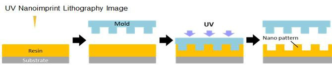
Examples of pattern fabrication using nanoimprint lithography
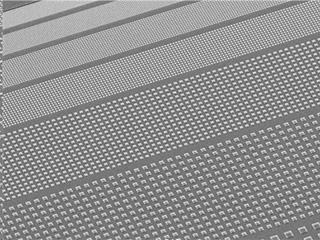
Width: 0.5-5μm, Depth: 350 nm
For purchases or inquiries, please contact us via the inquiry form.
Outside of Japan, sales may be prohibited in some countries due to laws and regulations concerning chemical substances.
For information on overseas distributors, please check here.
Distributors List